Leading solutions for CAM / DFM / 3D software
Validate data, detect issues earlier, and deliver clean manufacturing output with confidence.
Turn Your PCB Design Time Into Production Time
Engineers using our tools ship faster, with fewer manufacturing delays.
Become the Engineer Everyone Depends On
You'll be the one who can convert, prep, verify, and deliver data — fast.
Your Designs Won't Just Look Good — They'll Get Built
Manufacturing success is where careers are made. We bridge that final 10%.
Prevent Fabrication Errors Before They Happen
Validate data, detect issues earlier, and deliver clean manufacturing output with confidence.
Become a Better Engineer Tomorrow — Not Months From Now
No long training. No stress. Instantly practical skills that translate to real output.
Turn "DFM Anxiety" Into Production Confidence
You'll stop wondering if a board will build — and start knowing it will.
Your Manufacturing Partner Will Actually Love Your Files
Because you'll hand off clean, consistent, correct data every time.
Our Software Products
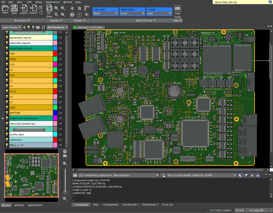
FAB 3000
The Ultimate CAM Tool for PCB Manufacturing
- ✓Advanced DFM analysis
- ✓Gerber, ODB++ IPC-2581 support
- ✓Export Assembly and drill data
- ✓Panelize PCBs
- ✓Build Centroids
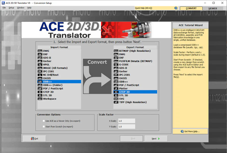
ACE 2D/3D Translator
CAD Conversion Tool
- ✓Convert DWG, DXF, STEP
- ✓Simplify and repair CAD files
- ✓Translate to Gerber, GDSII, 3D
- ✓ODB++, IPC-2581, PDF, Images, STL, TIFF, Bitmap
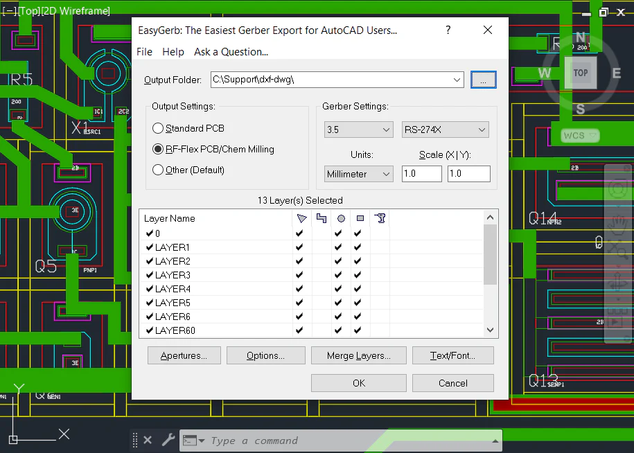
EasyGerb for AutoCAD
Instant Gerber Output from AutoCAD
- ✓Export AutoCAD layout to Gerber
- ✓No DXF or DWG files needed
- ✓Seamless integration with AutoCAD
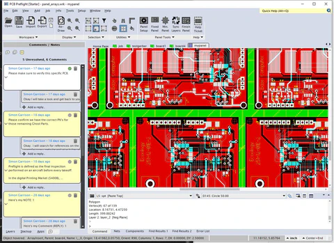
PCB Preflight – Free Viewer
Free Online Gerber Viewer with Collaboration
- ✓View Gerber, ODB++, IPC-2581
- ✓3D PCB Preview
- ✓Online Collaboration
- ✓Add Comments & Markup
- ✓Export to PDF
Engineers worldwide depend on our software solutions and dedicated technical support
We became a leader in the EDA software industry by empowering electronic designers and engineers with clever, high quality software tools which facilitate their designs for manufacturing.
Major Companies Embrace Numerical Innovations


What Our Customers Are Saying
"FAB 3000 ALWAYS works, even when other programs don't. Your software ROCKS!! So does the support. Wanted you to know how much I appreciate the excellent product and support."
Russell Steiner
Amtech Electrocircuits
"FAB 3000 is a great product. It more than stacks up against the competition, it is truly a notch above providing features such as sophisticated panelization that I only got with an expensive software - and even wasn't as capable as FAB 3000. Combine what is a superior product with the top notch, responsive support that Numerical Innovations provides, and you have a winning combination!"
Neil Szuminsky
Necessity Consulting
"I have created and converted 15 ACAD files to date with no issues thus far. EasyGerb is indeed very fast and easy to use just as the name implies. An actual conversion takes only seconds... I am especially pleased that in less than 3 weeks our data conversion cost savings have already offset 60% of our investment cost."
Dan Hughes
Towne Technologies Inc.
"ACE 3000 worked perfectly. I translated a gerber file to a DXF. I normally do board design in Mentor's PADs product and it has a miserable DXF translator. ACE 3000 worked great in this application."
Carol Henley
Xilinx
"I advocate to the students and staff the idea of using a vector illustrator like CorelDraw and Adobe Illustration to design a board layer. I have been doing it this way for almost 20 years. Your beautiful tool, FAB 3000 imports eps files of each layer and converts them to gerber flawlessly."
Michael E. Fleming
Portland State University
"EasyGerb did exceed my expectations as it did exactly what I wanted and it was simple to use and a small program to install within AutoCAD."
Rise Chang
QinetiQ
Numerical Cloud Subscriptions
Get All Desktop Software Tools for one low price!
1-Person
Up to
1
User
5-Person Team
Up to
5
Users
10-Person Team
Up to
10
Users
Receive a single Activation Code that runs our desktop software products, anywhere worldwide, across unlimited computers. Get full access to the latest releases plus technical support, on a low-cost subscription basis. Numerical Cloud is the perfect cost-effective solution for individuals, corporations, and universities.
Numerical Cloud: Get All Desktop Software Tools for one low price!
* Ready? Subscribe Now and instantly receive an email with your new activation code plus all software download links.
Ready to Get Started?
Experience the power of professional CAM / CAD / DFM / 3D software. Download our free demo and start running verification checks on your PCB designs today.